Specifications
Optical and electrical performance
Index Name | Typ |
Response spectrum (μm)*1 | 1.00 ±0.05~1.85 ±0.05 |
Pixel filling rate(%) | 100 |
Peak quantum efficiency (%) | ≥75 |
Peak detection rate(cm●Hz/ W) | ≥1×10¹² |
Peak sensitivity (A/W) | ≥0.8 |
Effective pixel rate (%)*2 | A line≥99,Other line≥99.5 |
Response inconsistency (%) | <5 |
playback mode | IWR 、ITR,optional |
Readout rate (MHz) | unipath≥10 |
Maximum frame rate (fps) | >20k |
Gain gear | 8 |
Saturation voltage (V) | 1.6 |
Conversion gain (nV/e-) | Gain gear 1:16000 Gain gear 2:8000 Gain gear 3:4000 Gain gear 4:2665 | Gain gear 5:1775 Gain gear 6:840 Gain gear 7:325 Gain gear 8:160 |
Notice:
*1 Focal plane temperature=25℃
*2 The deviation between the pixel response signal and the average value is less than a certain range's the percentage of pixels.
Response spectrum(TYP)

Schematic diagram of detector working principle and connection mode

Mechanical capacity
Terms | TYP |
Length x width x height (mm) | 28 × 15 × 6.2 |
Weight (g) | ~9 |
Focal Plane Scale | 512 × 2 |
Pixel Center Distance (μm) | 25 |
Pixel Size (μm) | 25 ×25 |
Sensing Area (mm) | 12.8 ×0.25 |
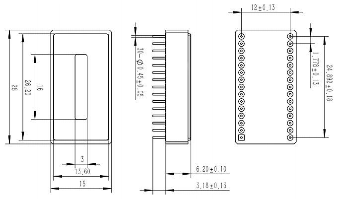
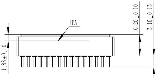
Dimensions and Pin definitions
Mechanical Specifications
The detector is packaged In ceramic form, filled with atmospheric pressure high purity nitrogen, the shell is made of alumina ceramic, the cover plate and pin are made of FeNiCoSi alloy, the surface is electroplated Ni/Au layer, the window welding is IN brazing, and the cover is resistance welding. The dimensions of the detector are 28mm (L)×15mm (W)×6.2mm (H). There are 30 pins with Φ0.45mm leading from the back on the shell, and the spacing of the pins is 1.778mm. They are used for the input of focal plane power supply and instruction, the electrical extraction of focal plane detection signal and temperature sensor, and the power input of thermoelectric refrigerator.
The appearance and size of mechanical interface are shown in the figure below.
Optical configuation
This product adopts 512×1 InGaAs focal plane which has two redundant elements at the left and right ends,the overall number of pixels is 516×1.Columns 3 to 514 are recommended for actual use.The shape of the pixel is rectangular, and the photosensitive size is 25μm×250μm.The structure is arranged in a "一" shape, and the pixel center distance is 25μm.The structure is shown in the figure below.
The design distance between the detector's photosensitive surface and the upper surface of the packaging structure is 1.86±0.1mm, the design distance between the photosensitive surface and the lower surface of the window is 1.16 ± 0.1mm,the design distance between the photosensitive surface and the mounting surface or the bottom of the tube shell is 4.34±0.1mm.The window material is sapphire,the thickness is 0.5±0.05mm the window refractive index is 1.76,the surface is coated with AR film,the transmittance in the response band>95%,and the window transmittance area is 16mm×3mm.The center of the photosensitive surface is located at the center of the detector,and the relative position deviation≤0.05mm,rotation displacement≤0.02mm.
Schematic diagram of detector pins
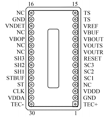
Pin Names | Input/Output | Pin function | Reference value |
GND | Input | ground wire | Working current<10mA |
CLK | Input | A clock that provides a time reference for circuit driven timing | Digital voltage;
High level 3.3V, low level 0V |
VDDD | Input | Digital circuit power supply, providing voltage to the digital circuit in the detector | Dc 3.3V, working current needs to be<5mA |
VDDA | Input | An analog circuit power supply that provides voltage to the analog circuit in the detector | Dc 3.3V, working current needs to be<25mA |
SC1 、SC2、 SC3 | Input | Detector gain selection, control detector output signal size, the control method is detailed in the timing section | Digital voltage
High level 3.3V, low level 0V |
ST | Input | Trigger the pulse, and the circuit begins to collect signals | Digital voltage
High level 3.3V, low level 0V |
RESET | Input | Reset the signal and control the length of the circuit acquisition cycle. See the timing section for the control method | Digital voltage
High level 3.3V, low level 0V |
SH1 、SH2、 SH3 | Input | Sample the control signal, set the pixel integration time, and change the readout mode. See the time sequence section for the control method | Digital voltage
High level 3 3V, low level 0V |
Pin Names | Input/Output | Pin function | Reference value |
VBOUT | Input | Buffer offset to provide the bias voltage for the total buffer of the circuit | DC2.3V |
VBOP | Input | The amplifier is biased to provide the bias voltage for the signal amplifier | DC2.3V~2.5V ,Recommend 2.4V |
VREF | Input | Reference voltage, which provides a reference value for the output signal | DC2.3V |
VNDET | Input | Chip common N | DC2.3V |
VBUF | Input | When in use, short connect with VBOUT pin | DC2.3V |
STBUF | Input | When used, it should be short connected with the ST pin | Digital voltage
High level 3.3V, low level 0V |
VOUTR | Output | Reference signal | 0.5V~2.5V |
VOUTS | Output | The output signal is subtracted from the reference signal of the same channel to obtain the actual detector response signal value | 0.5V~2.5V |
TS | - | The temperature sensor measures the resistance value through two pins to feedback the operating temperature of the focal plane |
|
TEC+、TEC- | - | The input voltage of the thermoelectric refrigerator is + pin for refrigeration when connected to high potential, and for heating when connected to low potential Empty foot | The rated voltage and current of TEC shall not be exceeded |
NC | - | The input voltage of the thermoelectric refrigerator is + pin for refrigeration when connected to high potential, and for heating when connected to low potential Empty foot |
|
Notice:
The DC input directly affects the overall noise of the detector, so the ripple noise of the DC input power supply has the following requirements:
1) VDDA<2mV
2) VDDD<10mV
3) VREF, VNDET<0.3mV
4) VBOP, VBOUT<1mV