- Home
- Support
- Technology
- Contact Us
- Solutions
- Product List
- Laser diodeSub
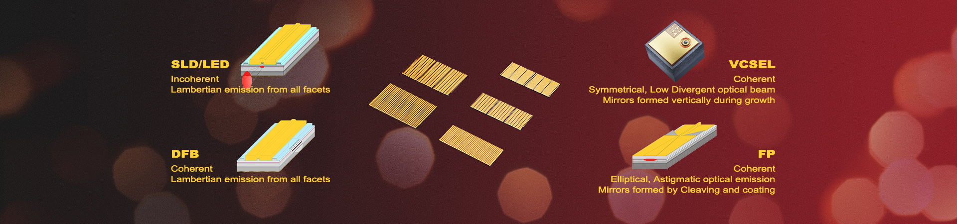
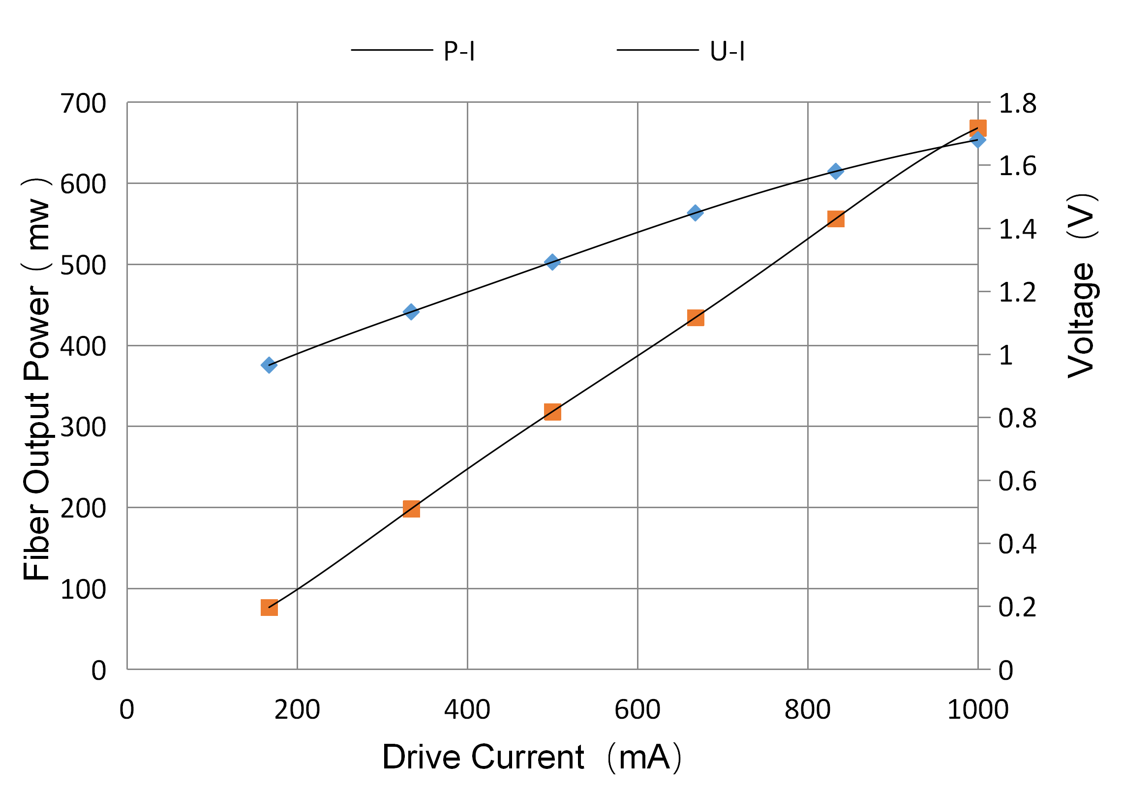
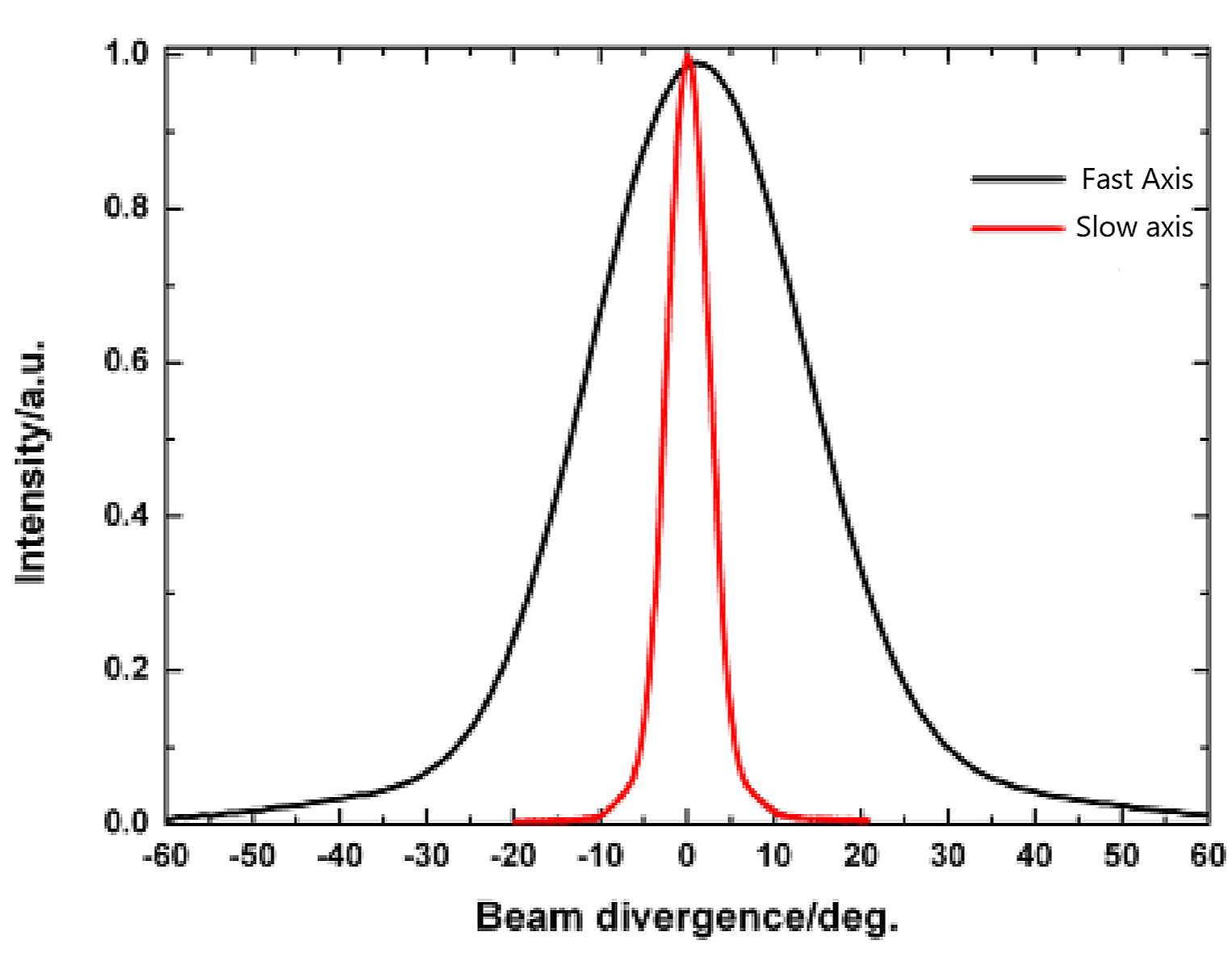
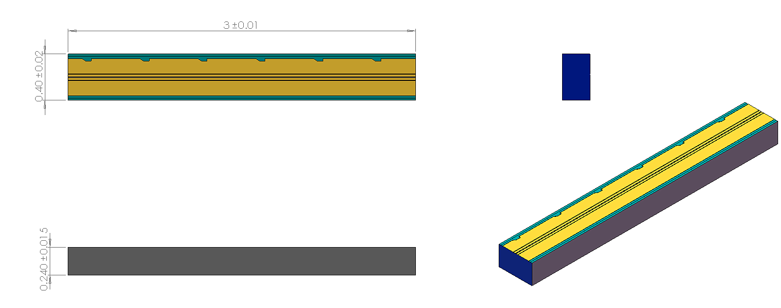
Laser diode
- Distributed Bragg Reflector LaserSub
- RF ModuleSub
- Distributed Feedback LaserSub
Distributed Feedback Laser
- Fabry-perot LaserSub
Fabry-perot Laser
- Light Emitting DiodeSub
Light Emitting Diode
- Superlum Laser DiodeSub
Superlum Laser Diode
- VCSEL Laser DiodeSub
VCSEL Laser Diode
- External Cavity LaserSub
External Cavity Laser
- Semiconductor Optical AmplifierSub
Semiconductor Optical Amplifier
- PhotodiodeSub
Photodiode
- InGaAs PDSub
InGaAs PD
- InGaAs APDSub
InGaAs APD
- InGaAs Single-Photon Avalanche Diodes (SPADs)Sub
InGaAs Single-Photon Avalanche Diodes (SPADs)
- InGaAs linear detectorSub
- InGaAs 2D array detectorSub
InGaAs 2D array detector
- InGaAs Microwave ReceiverSub
- SI PhotodiodeSub
SI Photodiode
- Si APDSub
- Si Quadrant PhotodiodesSub
Si Quadrant Photodiodes
- Special PhotodiodeSub
Special Photodiode
- Ge PhotodiodeSub
- InGaAs PDSub
- Light SourceSub
Light Source
- DFB Light SourceSub
DFB Light Source
- FP Light SourceSub
FP Light Source
- Broadband Light Source (ASE/SLD)Sub
- Pulse Fiber SourceSub
Pulse Fiber Source
- Narrow Linewidth Laser ModuleSub
Narrow Linewidth Laser Module
- Tunable Laser SourcesSub
- Swept Wavelength Laser SourceSub
Swept Wavelength Laser Source
- DFB Light SourceSub
- Detector moduleSub
Detector module
- InGaAS PD ModuleSub
InGaAS PD Module
- InGaAs APD ModuleSub
- InGaAs BPD ModuleSub
- InGaAs BAPD ModuleSub
InGaAs BAPD Module
- Si PD ModuleSub
- Si APD ModuleSub
- Si BPD ModuleSub
- Si BAPD ModuleSub
Si BAPD Module
- InAsSb PD ModuleSub
- HgCdTe PD ModuleSub
HgCdTe PD Module
- InGaAS PD ModuleSub
- Laser systemsSub
Laser systems
- Fiber Optical AmplifierSub
Fiber Optical Amplifier
- TDLAS Instrument Sub
- Test InstrumentsSub
- Fiber Optical AmplifierSub
- Laser accessoriesSub
Laser accessories
- Optical ComponentsSub
Optical Components
- Electrical ComponentsSub
Electrical Components
- Ultrafast OpticsSub
Ultrafast Optics
- RF AccessoriesSub
- Optical AccessorySub
- Optical ComponentsSub
- Laser ChipSub
Laser Chip
- CustomizeSub
Customize
- Photodiode CustomizeSub
Photodiode Customize
- Laser diode CustomizeSub
Laser diode Customize
- Photodiode CustomizeSub